Stiffness Tuning Using Nonlinearity in MEMS Sensors
Introduction
Nanomechanical sensors have emerged as powerful tools for detecting surface stress changes at the nanoscale. Their unparalleled sensitivity and precision have paved the way for advancements in fields such as material science, biology, and medicine. However, accurately modeling their behavior, particularly when dealing with nonlinearities, can be intricate. This tutorial delves into the process of modeling the nonlinear mechanical behavior of these sensors using Finite Element Analysis (FEA) in COMSOL. It serves as a foundational guide to understanding the modeling and implementation of the thin film-based stiffness tuning methods.
Understanding Sensor Behavior
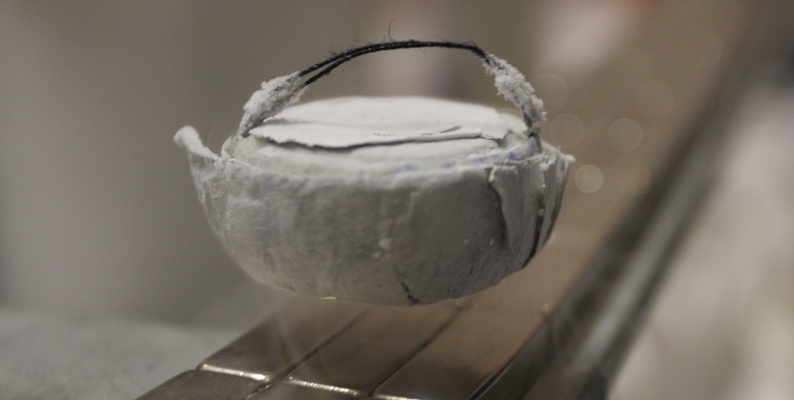
Nanomechanical sensors consist of two primary layers: the immobilization layer, often made of gold or polymer, and the silicon layer. When the immobilization layer interacts with external molecules, it can cause a strain mismatch with the silicon layer. This mismatch is associated with the surface stress in the layer, which causes the silicon layer to bend, producing piezoresistive signals at the embedded piezoresistor. These signals can then be harnessed to quantify the extent of the chemical interaction. An example can be found here.
The sensor performance can be enhanced by manipulating its stiffness. One effective method involves introducing prestress into the sensor using a highly stressed thin film. While tensile prestress can increase the device’s stiffness, as seen in the fabrication of resonantors with high natural frequency, compressive prestress can reduce the stiffness, enhancing its sensitivity to surface stress-induced bending.
Setting Up the Model
Geometry
This model is built using COMSOL Multiphysics 6.1. The .m file of the model can be found in this repo and it can be built through MATLAB Livelink.
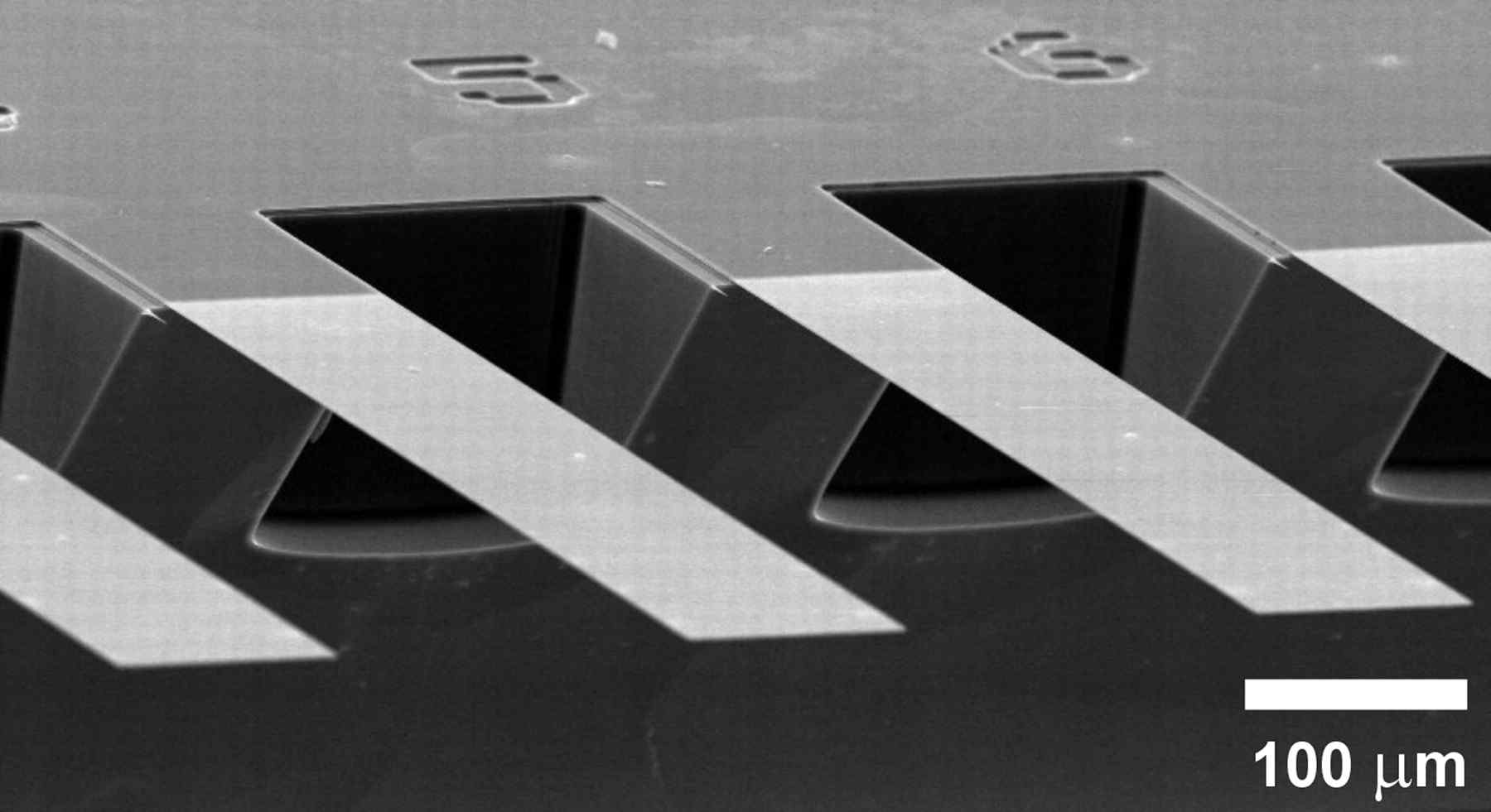
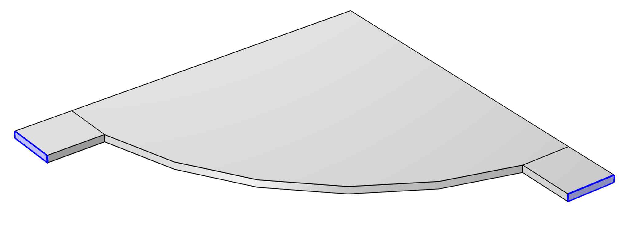
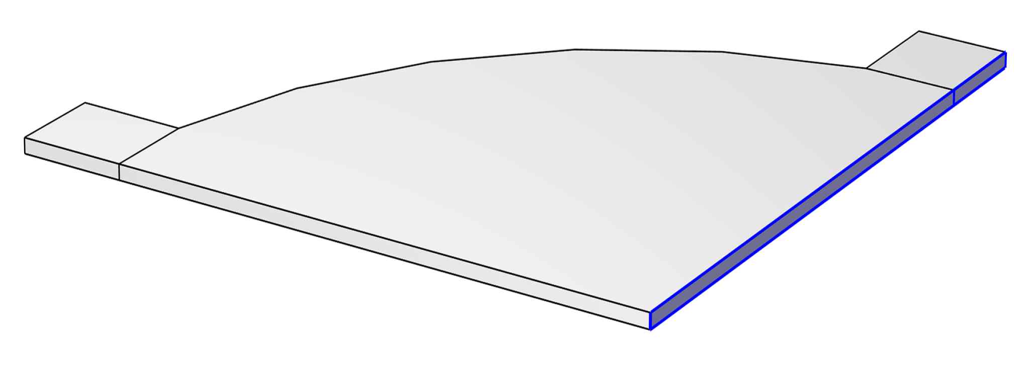
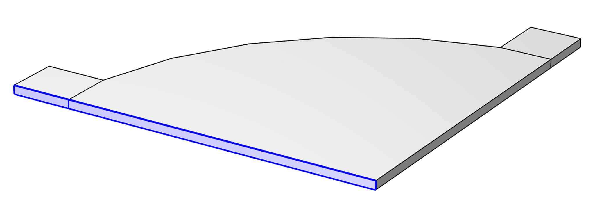
Our focus will be on the membrane-type surface stress sensor (MSS), which serves as a demonstration in this paper. This sensor features four piezoresistive sensing beams linked to a suspended silicon membrane, both having a thickness of 3 microns as modeled by the solid mechanics interface.
The immobilization layer is represented using a shell interface on the sensor surface, with its implicit thickness defined under the “Thickness and Offset 1” node. The solid and shell interfaces are coupled through a multiphysics node with a “shared boundaries” connection type.
The piezoresistors that are crucial for sensor performance evaluation are modeled as a smaller rectangle within the sensing beam, and it is also only defined at the sensor surface. The thickness of the piezoresistor is ignored for simplicity.
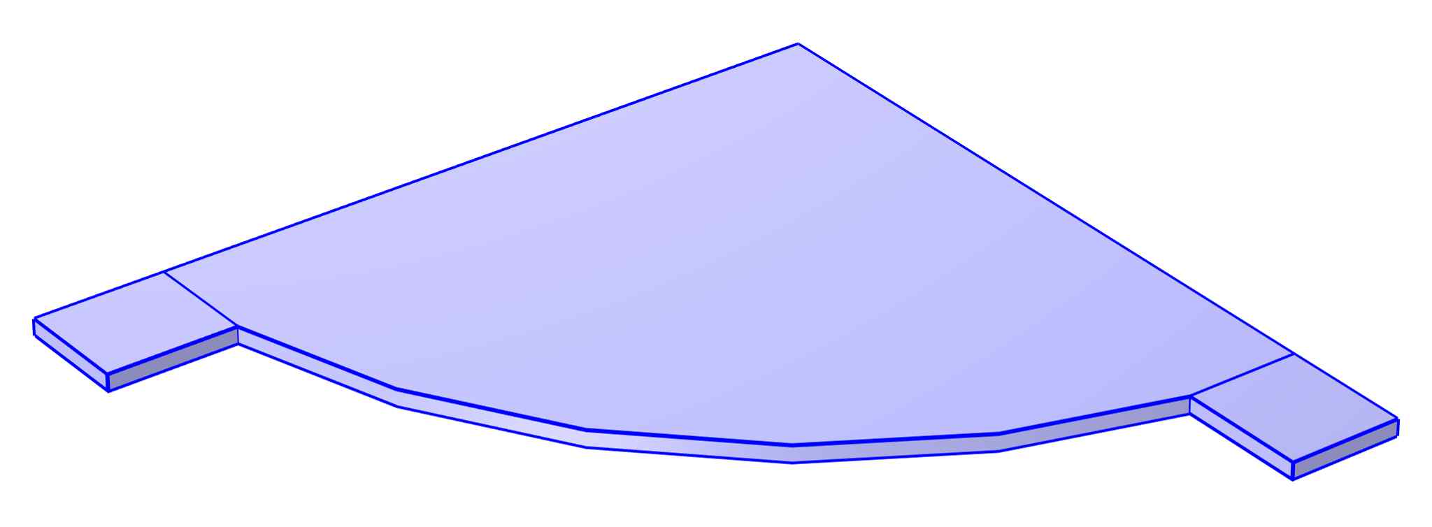
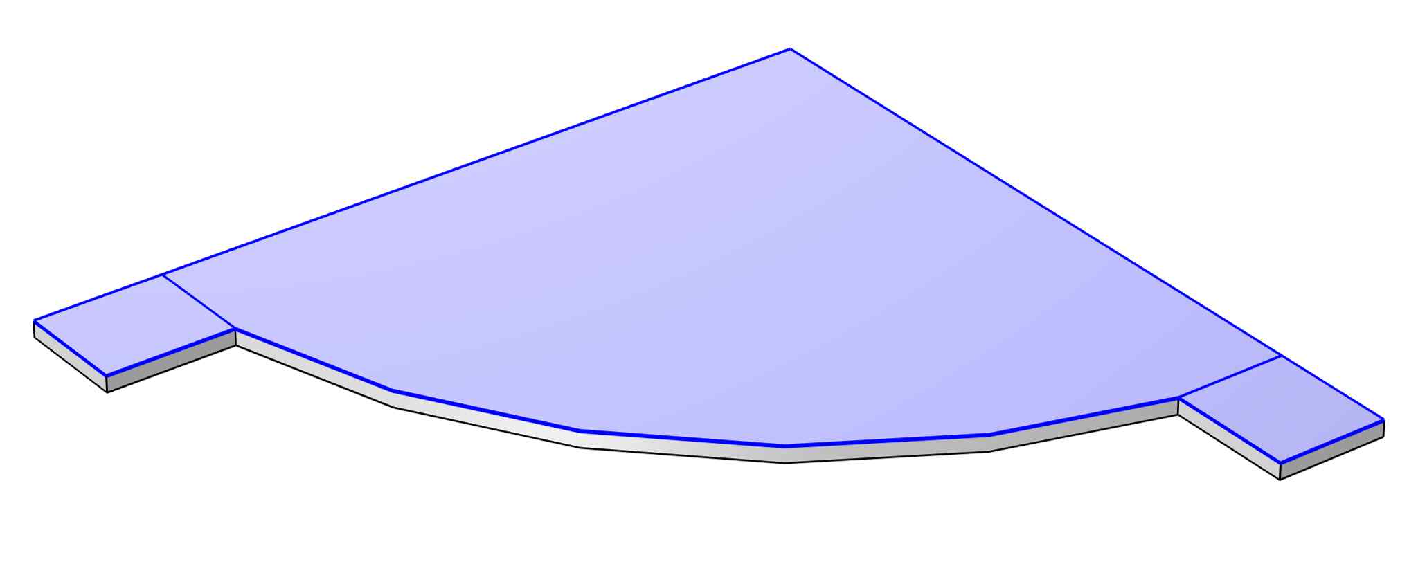
Due to the symmetrical design of the sensor, only a quarter of its geometry is modeled for efficiency.
Material Properties
The elasticity of silicon can either be modeled by specifying Young’s modulus and Poisson’s ratio or more explicitly by the elasticity matrix, through which one can have a better description of the anisotropy in silicon. But usually, Young’s modulus will suffice.
For the immobilization layer, we assume materials like gold or polymers exhibit isotropic behavior on silicon. Thus, their elasticity is defined using Young’s modulus and Poisson’s ratio.
Boundary Conditions
The end of four piezoresistive sensing beams are fixed, and the two-fold symmetry is specified by two symmetry nodes.
Load condition
The surface stress of the immobilization layer is defined by biaxial stress in the “Initial Stress and Strain” node under the “Linear Elastic Materials” at the shell interface.
The prestress of the silicon layer, on the other hand, is modeled as a biaxial prestrain at the same node in the solid mechanics interface. The reason for using strain is simplicity, that is, to avoid adding explicitly two layers of stressed thin films. As the desired effect is the strain in the silicon, we here directly implement them as prestrain instead of converting them back and forth through thin film stress.
Additionally, a “Global Equations” node is used in the solid mechanics interface to implement a displacement control scheme. This is a numerical trick to deal with the strong nonlinearity in the problem to avoid divergence, especially when snap-through instability is involved. A COMSOL tutorial can be found here.
Meshing the Model
The mesh is relatively simple: A quadrilateral mesh swept operation through the thickness direction. For better accuracy, one may assign different mesh sizes in the piezoresistor and the membrane.
Solving the Model
Check the “Include geometric nonlinear” at the top section to capture the geometric nonlinearity in the problem, which is required to calculate the change in stiffness when introducing prestress in the silicon layer. An explanation of geometric nonlinearity in COMSOL can be found here.
Moreover, the “Auxiliary sweep” is enabled. This sweep calculates the sensor deformation under increasing surface stress. Moreover, the prestress is slowly ramped up from zero to illustrate the effect of geometric nonlinearity.
With everything set up, run the FEA simulation. Because of the nonlinearities involved, this might take some time.
Post-processing and Analysis
First of all, let’s make an animation.
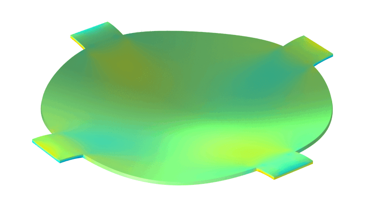
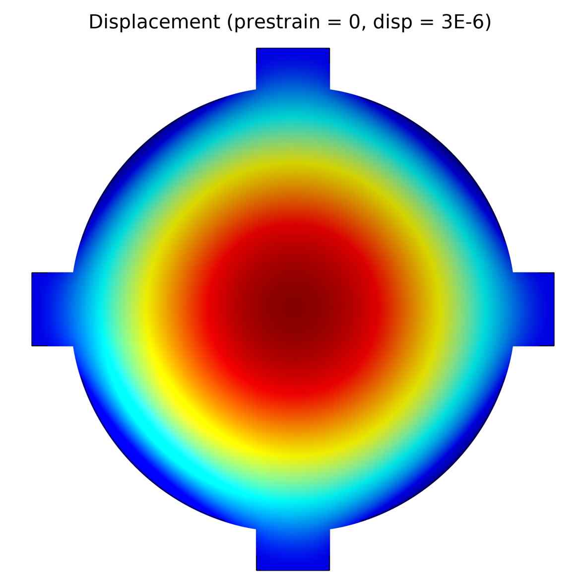
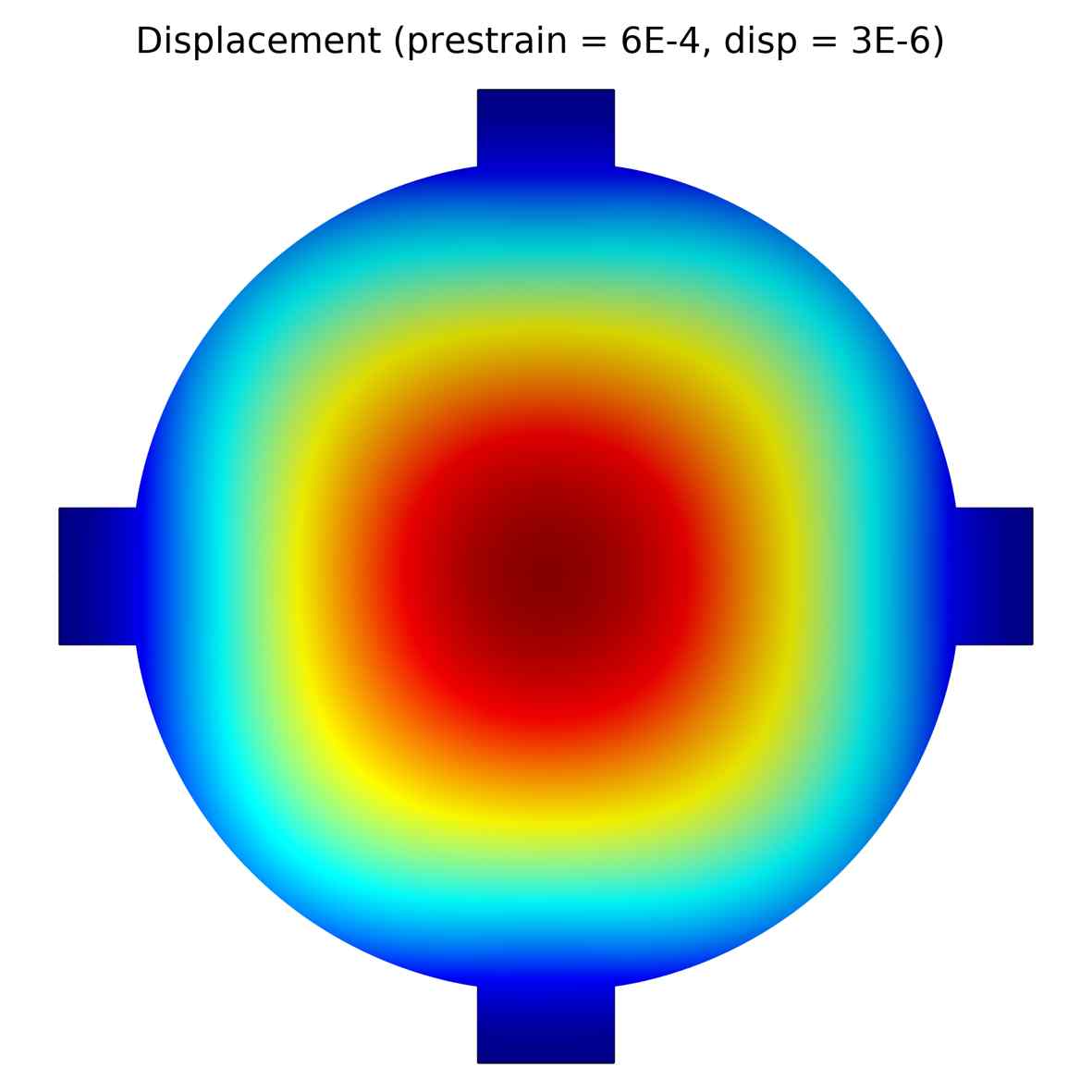
Once the simulation is complete, one can look at the displacement profile of the sensor. The membrane deforms differently depending on the level of prestrain in the silicon. When there is no prestrain, the profile contour is circular; when there is a high prestrain, the profile contour is a square shape.
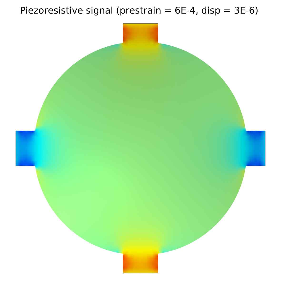
The piezoresistive signal profiles are similar with signals concentrated at the piezoresistor as one intended. Under the same deformation, the signal is stronger for the case with no prestress. This is because it is under a higher surface stress loading to reach this deformation state due to the high original stiffness. When there is prestress, the sensor is softened, and it can deform by 3 microns with a small surface stress, therefore, it exhibits a weaker piezoresistive signal at this state.
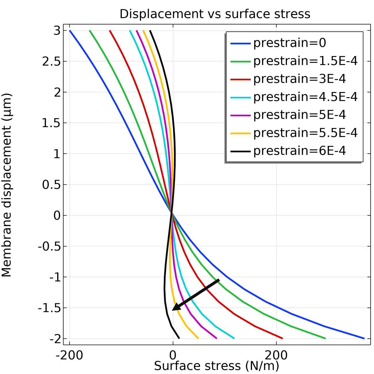
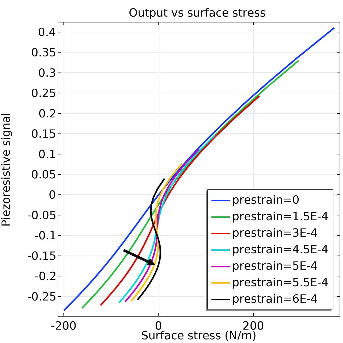
The following line graphs show the dependence of sensor deformation and piezoresistive signal as a function of surface stress under different prestress levels. As prestress increases, both curves become increasingly nonlinear, where the stiffness of the sensor transits from positive to negative values, entering post-buckling regimes. The increasing slopes at the inflection points indicate that the sensor stiffness decreases from positive to zero, and to negative as the prestrain/prestress increases, which is accompanied by a drastic change in sensitivity to surface stress. When the stiffness is zero, the sensor is buckled and the sensitivity goes to infinity, above which the sensor will exhibit snap-through instability as the stiffness reduces below zero.
Troubleshooting
If the solver does not converge, consider reducing the step size for prestress. A coarse mesh will also lead to convergence problems, so ensure it is refined enough to accurately model the deformation behavior.
See these two tutorials from COMSOL for more information about solving nonlinear static problems and the load ramping method.
If nothing works, consider reducing the number of parameters of the sweep. Try reducing the problem complexity to a point where it works, and then build the complexity up again after the issue is resolved.
Conclusion
Modeling the nonlinear behavior of nanomechanical sensors using FEA is a powerful approach to understanding their behaviors under high stress. With the understanding of stiffness control using thin film processes, one can now tackle the nonlinear aspect of mechanical modeling, allowing one to utilize nonlinearity and the associated post-buckling behaviors for better sensor designs.
Funding: This work is funded by the National Institute for Materials Science (NIMS) and the University of Tsukuba, Japan.