Beyond Trial-and-Error: A Systematic Approach to MEMS Sensor Design
Introduction
Microelectromechanical systems (MEMS) are integral to modern technology, enabling a variety of devices from microphones and pressure sensors to the micro-mirrors in projectors. Their small size makes them easy to integrate into compact spaces, and their low stiffness allows them to be highly sensitive to micro-scale interactions. One specialized MEMS sensor is particularly important for detecting surface stress, serving as the foundation for biosensors that can precisely identify DNA, RNA, and protein interactions.
Creating these highly sensitive surface stress sensors is no easy feat. While micro-cantilevers have been the go-to design for years, new designs often rely on a combination of educated guesses and trial-and-error, leaving many potentially useful designs unexplored. Here it enters topology optimization—a generative design method that allows us to create sensors that are both more effective and more efficient.
The Challenge
Creating an effective sensor is like solving a multi-variable optimization problem. We have to consider:
- What materials should we use?
- What should the sensor geometry be?
- How can we ensure manufacturability?
- How do we keep it cost-effective?
Our Approach
The topology optimization is performed using the optimization module in COMSOL multiphysics 6.1. For those unfamiliar with the method, I have written an introductroy blog post.
How Does the Sensor Work?
The sensor works like a “bimorph,” a structure made of two different materials. Imagine a “functional layer” that expands when it encounters specific stimuli. This functional layer is typically gold or responsive polymer. Below this layer is a silicon layer that doesn’t expand the same way. The difference in expanding behavior leads to a “strain mismatch” between the two layers.
To relieve this strain mismatch, the silicon layer bends, which leads to bending stress on a special component called a “piezoresistor.” This stress changes the electrical resistance in the piezoresistor, creating a measurable signal that tells us the sensor is reacting to something.
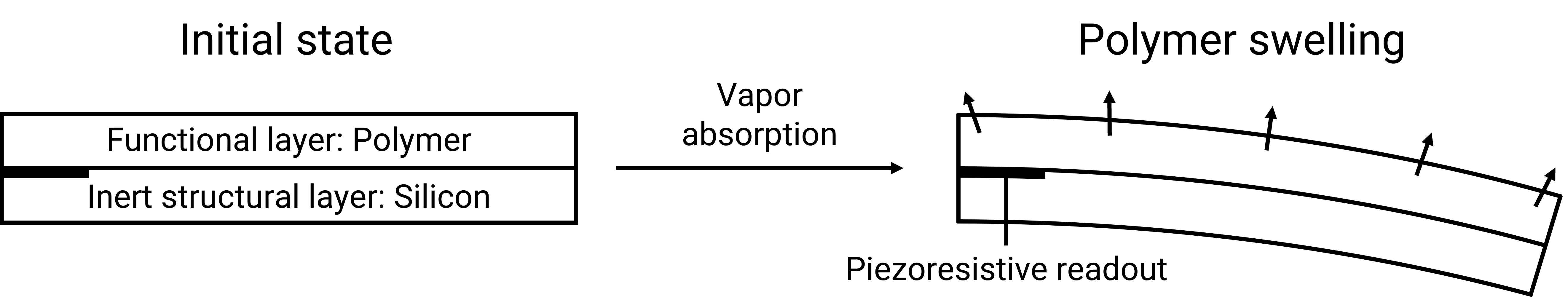
The key to a highly sensitive sensor lies in maximizing the stress on the piezoresistor. This is where traditional sensor designs often miss the mark, and it’s exactly what we aimed to improve with our optimized design.
Smart Design with Topology Optimization
Analysing 3D designs can be complex and time-consuming. So, we focused on optimizing a 2D layout of our sensor. This is implemented similar to a method used in a COMSOL tutorial. If you’re interested in the technical details, you can check out a tutorial post here for more information.
What Did We Find?
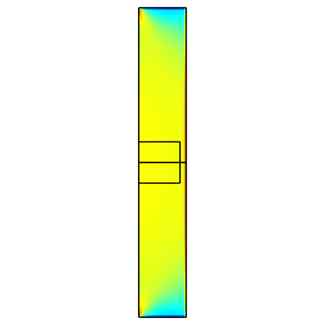
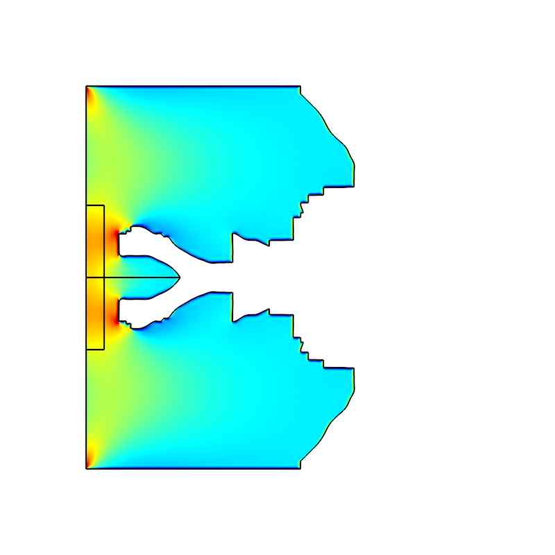
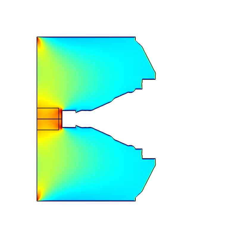
Our algorithm generated a design features with a double-cantilever, where the piezoresistor is at the intersection of two cantilever. This design diverges significantly from traditional designs where piezoresistor locates at the center of a single cantilever.
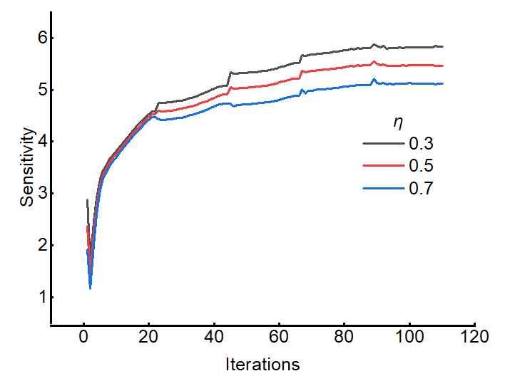
The optimization history is shown in the following figure. As the curves saturates at a large iteration numbers, we confirmed that our design has reached optimality.
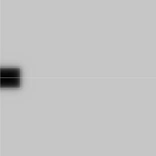
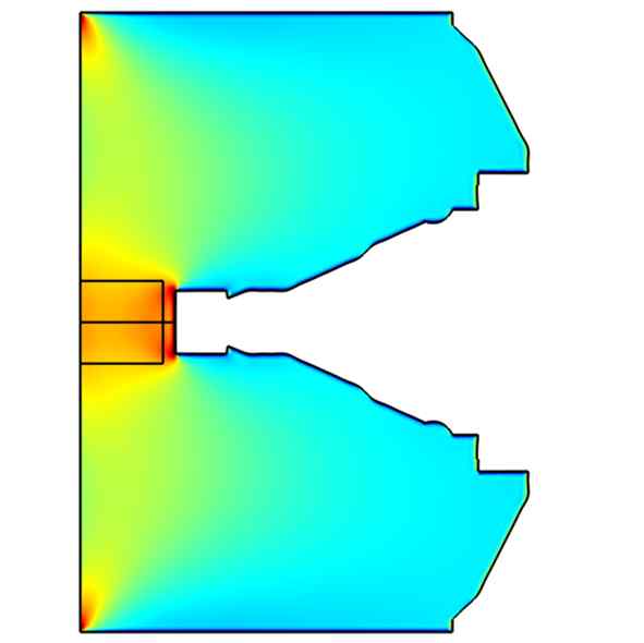
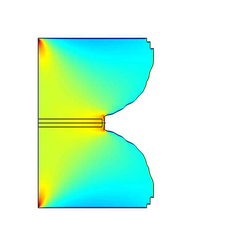
This special design gains its high sensitivity from the piezoresistor (the small black frame) being located at the region where drastic changes of bending cross-section occurs. The mismatch in bending behavior leads to the high stress at the well-positioned piezoresistor. The high performance can be seen from the distribution of piezoresistive signal between the optimized design and a conventional one, revealing a highly concentrated signal profile.
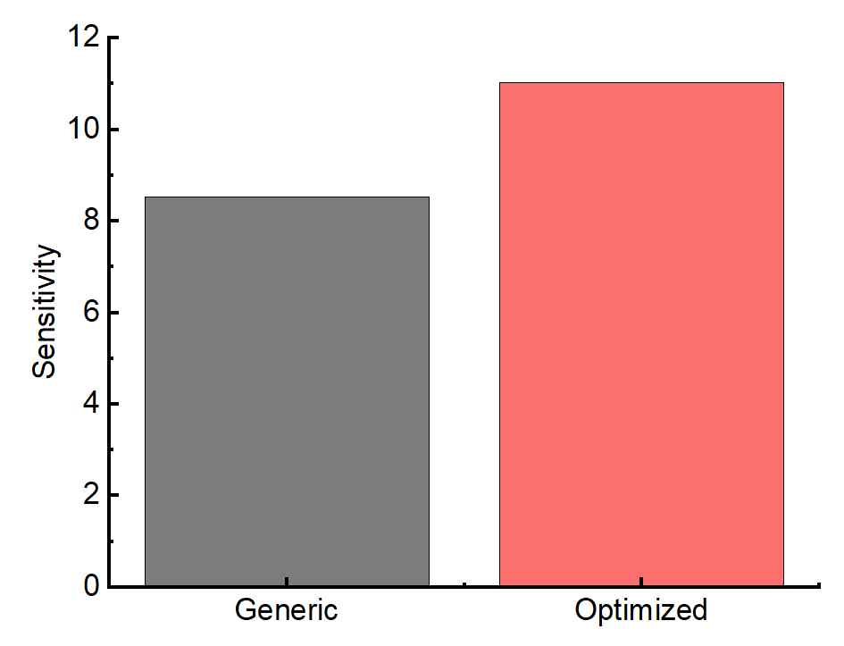
By comparing the sensitivity from two designs, we will find that the optimized design exhibit a significantly better performance compared to generic design, confirming the effectiveness of our optimization model.
This model is highly flexible—it can be expanded to include variations in geometric constraints, like the size and shape of the piezoresistor. For example, if one changes the aspect ratio of the piezoresistor, the optimized design will evolve accordingly. This allows for a systematic exploration of optimized designs under different fabrication constraints, helping us find the most efficient solution for surface stress sensing.
Additional Resources
Due to the nature of this COMSOL optimization workflow, which requires reimporting the optimized design into a second study within the same model (similar to a COMSOL tutorial here), generating a compact history .m file to describe the workflow is currently not supported by COMSOL. If you’re interested in accessing the .mph file, please feel free to contact either me or my supervisor.
In this optimization process, the internal slots for parametric sweeps are already used for parameter continuation and robust formulation. This makes it difficult to sweep over different geometrical constraints, such as the piezoresistor aspect ratio presented above. To address this issue, we use MATLAB LiveLink to automate the parameter sweep. The relevant code is available in this Github repository.
Wrapping Up
Topology optimization offers a powerful tool for designing piezoresistive sensors, allowing for more efficient and effective designs compared to traditional methods. Not only does this approach save time, but it also opens the door to novel designs that could revolutionize the field of MEMS devices. This model is just the starting point for a series of studies I’m working on. The model can be extended to include more complex materials like anisotropy (read more) or alternative boundary conditions, opening up new design possibilities.
Feel free to reach out with any questions or if you’re interested in collaborating on similar projects. Thank you for reading!
Funding: This work is funded by the National Institute for Materials Science (NIMS) and the University of Tsukuba, Japan.